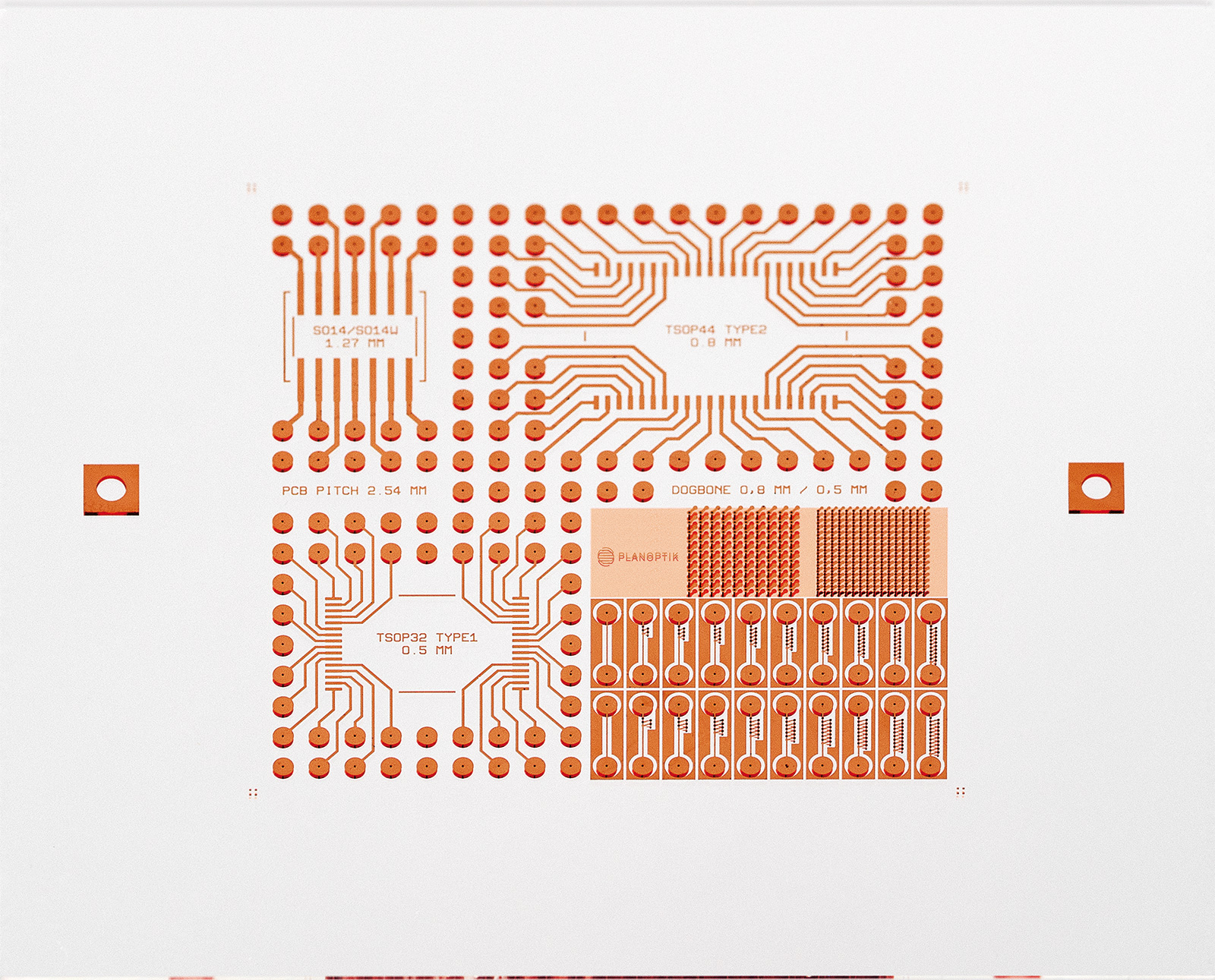
Mikroreaktoren und Mikrofluidiksysteme für chemische Prozesse in kleinen Volumina, einschließlich des Umgangs mit gefährlichen, sensiblen oder kostenintensiven Chemikalien und pharmazeutischen Wirkstoffen.
Source & evidence
Supplier website Mikrosysteme für Flow Chemistry – – Mikrofluidische Systeme, Reaktoren, Mikrodosierpumpen – – Mikroreaktoren und Mikrofluidiksysteme von PLANOPTIK ermöglichen chemische Prozesse in sehr kleinen Volumina, beispielsweise für den sicheren und effizienten Umgang mit gefährlichen, sensiblen oder kostenintensiven Chemikalien sowie pharmazeutischen Wirkstoffen. PLANOPTIK AG website Checked 17 Oct 2026
Glas schützt Licht- und Drucksensoren sowie andere Halbleiter; die Lösungen werden gemeinsam entwickelt und millionenfach auf Basis von Glaswafern gefertigt.
Source & evidence
Supplier website Wafer für Wafer-Level Packaging – – Chips und Sensoren geschützt durch Glas – – Licht- und Drucksensoren sowie andere Halbleiter mit Glas bedecken – gemeinsam entwickelt und millionenfach gefertigt auf der Basis von Wafern aus Glas. PLANOPTIK AG website Checked 17 Oct 2026
Wafer als Träger für die Bearbeitung ultradünner Wafer, angepasst an Produktionsprozesse in der Halbleiterindustrie.
Source & evidence
Supplier website Carrier Wafer, Adapter und Tools – – Unsere Wafer als Träger für die Bearbeitung von ultradünnen Wafern – – Wafer von PLANOPTIK sind angepasst an Ihre Produktionsprozesse in der Halbleiterindustrie. PLANOPTIK AG website Checked 17 Oct 2026
Glas-Substrate, mit denen Chips und Sensoren auf kleinstem Raum gestapelt werden können; individuell entwickelt.
Source & evidence
Supplier website Glass Core Substrates für Advanced Packaging – – Mikrochips und Sensoren optimal in elektronischen Geräten anordnen – – Glassubstrate ermöglichen das Stapeln von Chips und Sensoren auf kleinstem Raum. Individuell entwickelt. PLANOPTIK AG website Checked 17 Oct 2026
Microstructured components for diagnostics, biotechnology, medical technology and pharmaceutical applications.
Source & evidence
Supplier website Mikrostrukturierte Bauteile für die Diagnostik, Biotechnologie, Medizintechnik und pharmazeutische Anwendungen – – Komponenten für Life Science PLANOPTIK AG website Checked 17 Oct 2026
Microstructured parts for diagnostics, biotechnology, medical technology and pharmaceutical applications.
Source & evidence
Supplier website Microstructured parts for diagnostics, biotechnology, medical technology and pharmaceutical applications – – Microfluidic components for life science PLANOPTIK AG website Checked 17 Oct 2026
Glass substrates with through-connections and metallization for 3D integration, for advanced packaging.
Source & evidence
Supplier website Glassubstrate mit Durchkontaktierungen und Metallisierung für die 3D-Integration – – Glass Core Substrates für Advanced Packaging PLANOPTIK AG website Checked 17 Oct 2026
Glass substrates for advanced packaging, processed with through-glass vias and copper metallization.
Source & evidence
Supplier website PLANOPTIK develops Glass Core Substrates for advanced packaging, providing a high-precision platform for attaching and interconnecting microchips and semiconductor components. The glass core is processed with fine through-glass vias and copper metallization, enabling reliable routing and high-density electrical interfaces using wafer-level manufacturing and lithographic structuring. PLANOPTIK AG website Checked 17 Oct 2026
Customized wafers and panels for encapsulating MEMS and sensors; wafers for wafer-level packaging.
Source & evidence
Supplier website Maßgeschneiderte Wafer und Panels für die Verkapselung von MEMS und Sensoren – – Wafer für Wafer-Level Packaging PLANOPTIK AG website Checked 17 Oct 2026
Glass microreactors, micromixers and microdosing pumps for chemical and pharmaceutical processes.
Source & evidence
Supplier website Glass microreactors, micromixers and microdosing pumps for chemical and pharmaceutical processes – – Microfluidic systems for flow chemistry PLANOPTIK AG website Checked 17 Oct 2026
Glass microreactors, micromixers and microdosing pumps for chemical and pharmaceutical processes.
Source & evidence
Supplier website Glas-Mikroreaktoren, Mikromischer und Mikrodosierpumpen für chemische und pharmazeutische Prozesse – – Mikrofluidiksysteme für Flow Chemistry PLANOPTIK AG website Checked 17 Oct 2026
Customized wafers and panels for MEMS and sensor encapsulation.
Source & evidence
Supplier website Customized wafers and panels for MEMS and sensor encapsulation – – Wafers for wafer-level packaging PLANOPTIK AG website Checked 17 Oct 2026
Tools tailored to individual production processes.
Source & evidence
Supplier website Auf Ihren individuellen Produktionsprozess zugeschnittene Werkzeuge – – Carrier Wafer, Adapters und Tools PLANOPTIK AG website Checked 17 Oct 2026
Wafer aus Glas, Quarz und Silizium in Standardgrößen und -formen oder nach Kundenanforderungen, bis hin zur Serienfertigung.
Source & evidence
Supplier website Standard- oder massgefertigte Wafer – – Wafer aus Glas, Quarz und Silizium – – PLANOPTIK bietet ein breites Sortiment an hochwertigen Wafern aus Glas, Quarz und Silizium – in Standardgrößen und -formen mit kurzen Lieferzeiten direkt ab Lager oder maßgeschneidert auf die Anforderungen unserer Kunden bis hin zu deren Serienfertigung. PLANOPTIK AG website Checked 17 Oct 2026
Fully functional micro nozzles with structure sizes starting from 3 µm.
Source & evidence
Supplier website Examples include fully functional micro antennas, induction coils for sensors or fully functional micro nozzles with structure sizes starting from 3 µm. PLANOPTIK AG website Checked 17 Oct 2026
Supplier website Examples include fully functional micro antennas, induction coils for sensors or fully functional micro nozzles with structure sizes starting from 3 µm. PLANOPTIK AG website Checked 17 Oct 2026
Supplier website Examples include fully functional micro antennas, induction coils for sensors or fully functional micro nozzles with structure sizes starting from 3 µm. PLANOPTIK AG website Checked 17 Oct 2026
Trade-fair listing SEMICON Europa > Components, Parts & Accessories > Chucks for Wafer and other Substrates electronica 2026 exhibitor directory Checked 26 Sept 2026
Develops electronic, mechanical, optical, chemical or biological microcomponents using materials including glass, silicon and copper.
Source & evidence
Supplier website In us you will find a partner who will work with you to develop electronic, mechanical, optical, chemical or biological microcomponents and has a firm grasp of materials such as glass, silicon and copper. PLANOPTIK AG website Checked 17 Oct 2026
Fertigung von Mikrokomponenten
Fertigung gemeinsam entwickelter Mikrokomponenten und Elemente in großen Stückzahlen mit waferbasierten Fertigungsverfahren.
Source & evidence
Supplier website PLANOPTIK fertigt die gemeinsam entwickelten Mikrokomponenten und Elemente zudem in großen Stückzahlen unter Einsatz modernster waferbasierter Fertigungsverfahren. PLANOPTIK AG website Checked 17 Oct 2026
Medical-device component development
Develops components for medical devices using wafer-based production processes and plastics, including injection molding.
Source & evidence
Supplier website PLANOPTIK also develops components for medical devices, which are manufactured not only using wafer-based production processes but also using plastics, for example via injection molding. PLANOPTIK AG website Checked 17 Oct 2026
Manufacturing of jointly developed microcomponents
Manufactures jointly developed microcomponents and elements in high volumes using wafer-based manufacturing processes.
Source & evidence
Supplier website PLANOPTIK also manufactures the jointly developed microcomponents and elements in high volumes using state-of-the-art wafer-based manufacturing processes. PLANOPTIK AG website Checked 17 Oct 2026
Entwicklung von Mikrokomponenten
Gemeinsame Entwicklung elektronischer, mechanischer, optischer, chemischer oder biologischer Mikrokomponenten.
Source & evidence
Supplier website Bei uns finden Sie einen Partner, der gemeinsam mit Ihnen elektronische, mechanische, optische, chemische oder biologische Mikrokomponenten entwickelt PLANOPTIK AG website Checked 17 Oct 2026
Component and microcomponent development
Develops electronic, mechanical, optical, chemical or biological microcomponents with customers.
Source & evidence
Supplier website In us you will find a partner who will work with you to develop electronic, mechanical, optical, chemical or biological microcomponents and has a firm grasp of materials such as glass, silicon and copper. PLANOPTIK AG website Checked 17 Oct 2026
Consulting & technology transfer
Listed capability; detailed scope not provided.
Source & evidence
Trade-fair listing SEMICON Europa > Manufacturing Services or Consulting > Wafer Handling electronica 2026 exhibitor directory Checked 26 Sept 2026
Industries served
Semiconductor manufacturing
Source & evidence
Trade-fair listing SEMICON Europa > Components, Parts & Accessories > Chucks for Wafer and other Substrates electronica 2026 exhibitor directory Checked 26 Sept 2026
PLANOPTIK announced its participation and a presentation on glass core substrates and glass wafers for packaging.
Source & evidence
Supplier website We are very happy to participate in the IMPACT IAAC Conference! Our team will be at the there to connect with industry experts and discuss the latest developments in advanced packaging. We are also excited to contribute to the technical program with a presentation highlighting our glass core substrates and glass wafers for wafer-level and panel-level packaging. PLANOPTIK AG website Checked 17 Oct 2026
Semicon Europa Exhibition
PLANOPTIK announced that it will showcase glass substrates and wafers for semiconductor manufacturing and advanced packaging.
Source & evidence
Supplier website We are excited to announce our participation in SEMICON Europa! At our booth, we will showcase our range of glass substrates for semiconductor manufacturing, including carrier wafers, adapters and tools, as well as glass wafers for the encapsulation of MEMS and sensors. We will also present wafers and panels for advanced packaging applications. PLANOPTIK AG website Checked 17 Oct 2026
SPIE Photonics West Exhibition
The page lists PLANOPTIK's participation in SPIE Photonics West.
Source & evidence
Supplier website Advanced Glass Substrates Event SPIE Photonics West Exhibition …Event details to follow… Showcase products > Glass Wafers, Quartz Wafers & Silicon Wafers > Carrier Wafers, Adapters & Tools > Glass Core Substrates for Advanced Packaging PLANOPTIK AG website Checked 17 Oct 2026
Evidence & freshness
Every claim keeps its source. Company-reported information and independent verification are labelled separately. Spot something wrong? .
Supports 9 facts: Company name · Description · Mikrosysteme für Flow Chemistry · Wafer für Wafer-Level Packaging · Carrier Wafer, Adapter und Tools · Glass Core Substrates für Advanced Packaging · Standard- oder massgefertigte Wafer · Fertigung von Mikrokomponenten
Supports 8 facts: Company name · Microfluidic components for life science · Microfluidic systems for flow chemistry · Wafers for wafer-level packaging · Carrier wafers, adapters and tools · Components · Standard or customized wafers · Location: Elsoff, Germany
AI-inferred Based only on `company`, does this company offer engineering or product-design services for customers' products (hardware, firmware, PCB layout, product development)?
PCB fabricator · 60%Source & evidence
AI-inferred Based only on `company`, does this company fabricate bare printed circuit boards (PCB fabrication, not assembly)?
Contract manufacturer · 58%Source & evidence
AI-inferred Based only on `company`, does this company manufacture or assemble products for other companies as a service (EMS, contract manufacturing, OEM/ODM production, PCB assembly for customers)?
Machine shop / parts job shop · 27%Source & evidence
AI-inferred Based only on `company`, does this company machine or fabricate parts to customers' drawings (CNC machining, turning, sheet-metal job shop)?
System integrator · 15%Source & evidence
AI-inferred Based only on `company`, does this company build customer-specific turnkey systems by integrating equipment and components (for example automation cells, test systems, production lines)?